
Overview
Our research group is engaged in the research of atomic-scale interface physics, mainly interested in the study of thin-film heterointerfaces, crystal defects, and nanomaterial surfaces by electron microscopy. The main achievements so far include: (1) Invented a four-dimensional electron energy loss spectroscopy technique with both spatial and momentum resolution capabilities, realized the efficient mapping of phonon dispersion distribution at the nanoscale, and observed the phonon mode at the heterojunction interface. (2) Proposed a scheme to measure the far-infrared phonon polariton using electron microscope electron energy loss spectroscopy technology, and its momentum measurement range is increased by two orders of magnitude compared with nano-optics, which obtained the known The highest recorded compression ratio. (3) New phenomena such as flexoelectricity, antiferroelectric distortion, and spin valve of oxide defects were discovered, and new insights were put forward to explain their electrical activity. (4) We found lead-based ferroelectrics There is no intrinsic critical dimension in. (5) Cooperatively determined the polarization distribution of a single polar topological structure and revealed its evolution behavior under external fields, discovered polar topological antivortices in non-polar materials, expanded The research scope of polar topological materials. (6) Collaborated to systematically study graphene-based nitrogen in remote epitaxy and van der Waals epitaxy modes Chemical physics, materials, devices. |
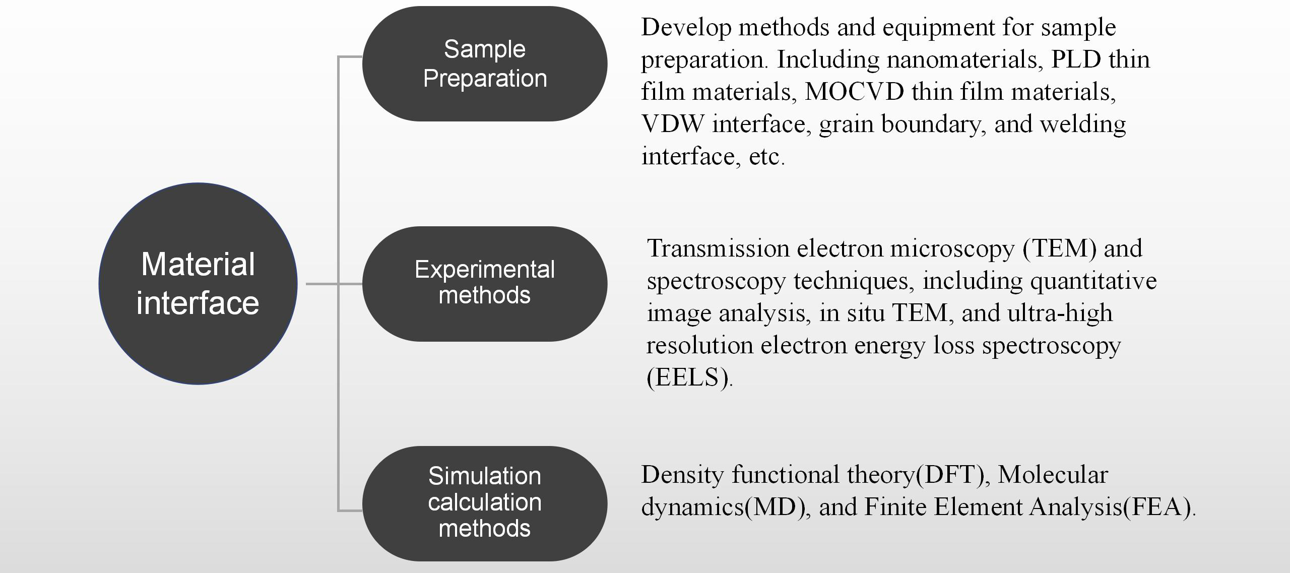
Research interests in Interface Lab
 |
Recent Highlights
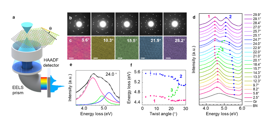
Tunable Interband Transitions in Twisted h-BN/Graphene Heterostructures
The randomly twisted heterostructures may also have unexpected transition behaviors, which may influence the device performance. Here, we study the twist-angle-dependent coupling effects of h-BN/grapheneheterostructures using monochromatic electron energy loss spectroscopy. Our findings indicate that twist-coupling effects of van der Waals heterostructures should be carefully considered in device fabrications, and the continuously tunable interband transitions through the twist angle can serve as a new degree of freedom to design optoelectrical devices. ( Physical Review Letters 131, 016201 (2023)) 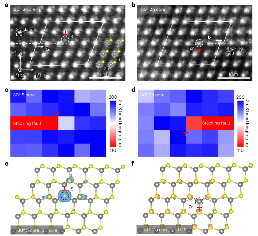
Harnessing dislocation motion using an electric field
Dislocation motion is critical for the hardening, processing and application of structural and functional materials. However, the goal of manipulating dislocation motion via a non-mechanical field alone remains elusive. Here we present real-time observations of dislocation motion controlled solely by using an external electric field in single-crystalline zinc sulfide-the dislocations can move back and forth depending on the direction of the electric field. We reveal the non-stoichiometric nature of dislocation cores and determine their charge characteristics. This study provides direct evidence of dislocation dynamics controlled by a non-mechanical stimulus and opens up the possibility of modulating dislocation-related properties. ( Nature Materials 22, 958-963. (2023)) 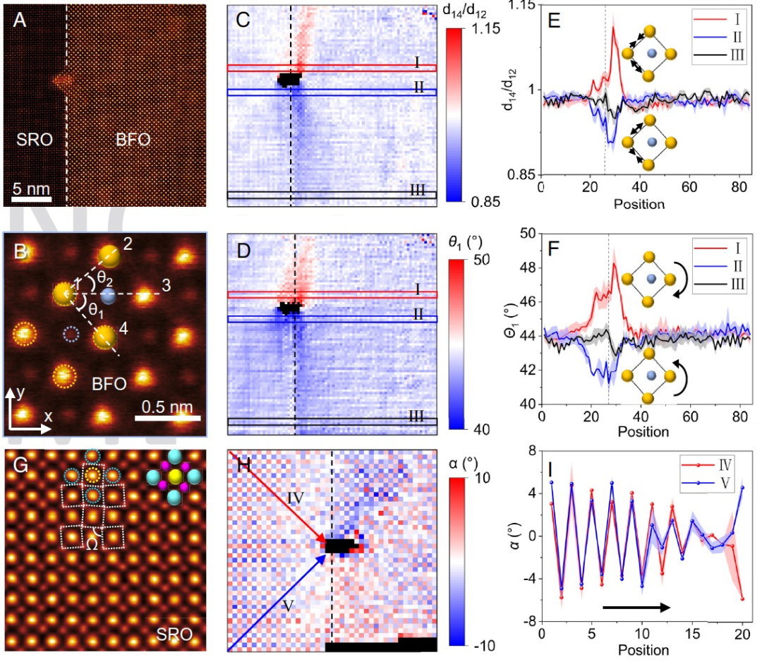
Dislocation-tuned ferroelectricity and ferromagnetism of the BiFeO3/SrRuO3 interface
In ferroelectric/ferromagnetic systems, misfit dislocations at the heteroepitaxial interface can significantly alter the local properties through strain-field-induced structural distortion. In this work, we use scanning transmission electron microscopy to unit-cell-by-unit-cell map the lattice parameters and octahedral rotations around misfit dislocations at the BiFeO3/SrRuO3 interface, and, thus, reveal the distinct effects of structural distortion on the local ferroelectricity and ferromagnetism properties. ( Proceedings of the National Academy of Sciences 120 (13): e2213650120 (2023)) 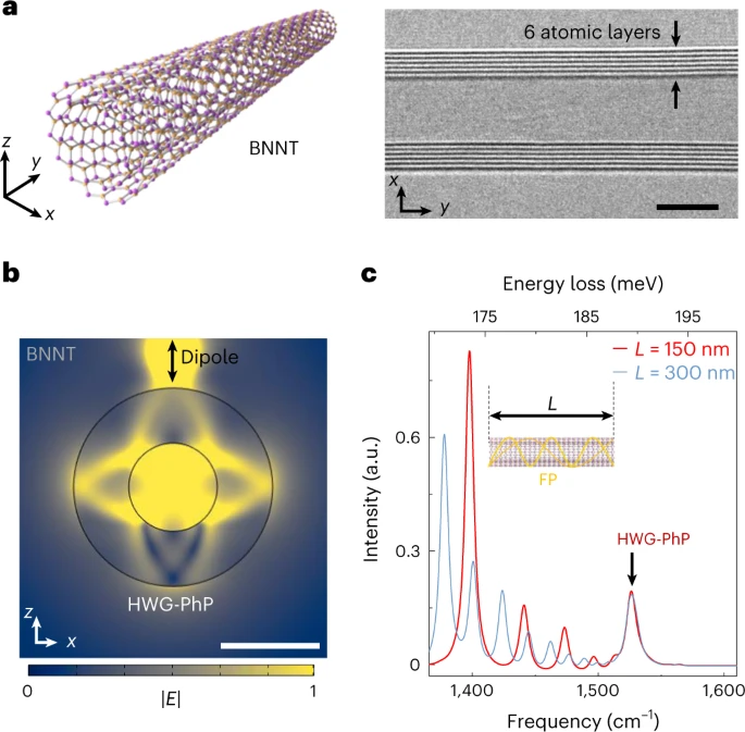
Hyperbolic whispering-gallery phonon polaritons in boron nitride nanotubes
Here, we show that hexagonal BN nanotubes act as an atomically smooth nanocavity that can sustain phonon-polariton whispering-gallery modes, owing to their intrinsic hyperbolic dispersion and low scattering losses.We posit that BN nanotubes could become an important material platform for the realization of one-dimensional, ultrastrong light–matter interactions, with exciting implications for compact photonic devices. ( Nature Nanotechnology 18:529-534 (2023)) 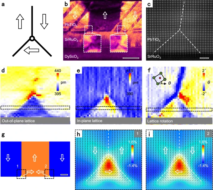
Electric-field control of the nucleation and motion of isolated three-fold polar vertices
Here, we show the controlled nucleation and motion of isolated three-fold vertices under an applied electric field. At the PbTiO3/SrRuO3 interface, a two-unit-cell thick SrTiO3 layer provides electrical boundary conditions for the formation of three-fold vertices. Microstructural evolution of the nucleation and propagation of isolated three-fold vertices is further revealed by phase-field simulations. This work demonstrates the ability to electrically manipulate isolated three-fold vertices, shedding light on the dynamic property of isolated topological polar structures. ( Nature Communications 13: 6340 (2022) ) 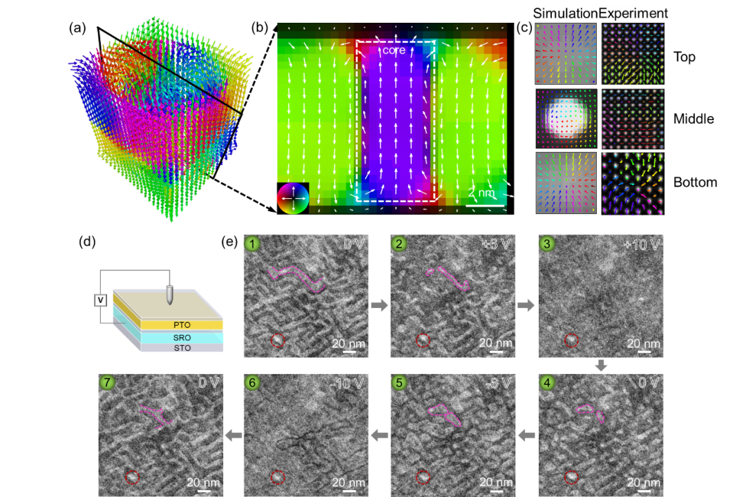
Dynamics of Polar Skyrmion Bubbles under Electric Fields
Herein, we study the dynamics of individual polar skyrmions at the nanoscale via in situ scanning transmission electron microscopy. By monitoring the electric-field-driven creation, annihilation, shrinkage, and expansion of topological structures in real space, we demonstrate the reversible transformation among skyrmion bubbles, elongated skyrmions, and monodomains. The underlying mechanism and interactions are discussed in conjunction with phase-field simulations. The electrical manipulation of nanoscale polar skyrmions allows the tuning of their dielectric permittivity at the atomic scale, and the detailed knowledge of their phase transition behaviors provides fundamentals for their applications in nanoelectronics. ( Physical Review Letters 129 (10), 107601 (2022) ) 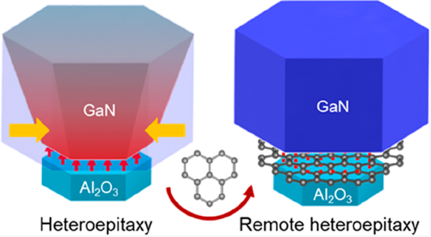
Remote Heteroepitaxy Using a Graphene Interlayer
We used graphene-assisted remote heteroepitaxy to achieve low-strain single-crystalline nitride films on highly mismatched (~16.3%) sapphire, which led to the in-plane compressive strain at the interface releases by 30%, and prevented the dislocations. And the density of edge dislocations in as-grown nitride films reduces to the same level as that of the screw dislocations. Besides, the indium composition in InxGa1–x/GaN multiquantum wells increases to ∼32%, enabling the fabrication of a yellow light-emitting diode. ( Nano Letters. (2022)) 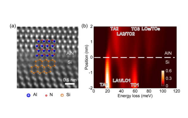
Atomic-Scale Probing of Heterointerface Phonon Bridges
Currently, there is a lack of effective experimental means to measure interface phonons. Recently, our group has demonstrated the measurement of phonon dispersion at the interface of heterojunction based on the technique of four-dimensional electron energy loss spectroscopy (Nature 2021, 559, 399). The spectroscopic method was used to measure the lattice dynamics of the interface between the third-generation semiconductor aluminum nitride (AlN) and silicon (Si) substrate, metal aluminum (Al) electrode, etc., and to explore the phonon transport at different interfaces. Behavior and its contribution to interfacial thermal conductance. (Proceedings of the National Academy of Sciences 119(8): e2117027119. (2022)) 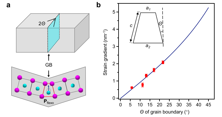
Atomic-scale flexoelectricity at grain boundaries
Large elastic deformations are generally difficult to achieve in most solids, and tiny strain gradients are difficult to control. We exploit the exotic structural inhomogeneity of grain boundary to achieve a huge strain gradient (~1.2 nm−1 ) within 3–4-unit cells, and thus obtain atomic-scale flexoelectric polarization of up to ~38 μC cm−2 at a 24° LaAlO3 grain boundary. We further demonstrate that varying the misorientation angle of the grain boundaries can achieve tunable strain gradients at the atomic scale for different materials. (Nature Communications 13(1): 216. (2022)) 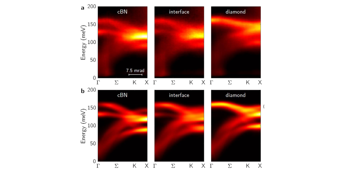
Measuring phonon dispersion at an interface
Interface phonons play an essential role in thermal/electrical transport properties in devices we use electron energy loss spectroscopy in an electron microscope to directly measure both the local phonon density of states and the interface phonon dispersion relation for an epitaxial cBN-diamond heterointerface. In addition to bulk phonon modes, we observe acoustic and optical phonon modes localized at the interface, and modes isolated away from the interface. (Nature 599(7885): 399-403.(2021)) 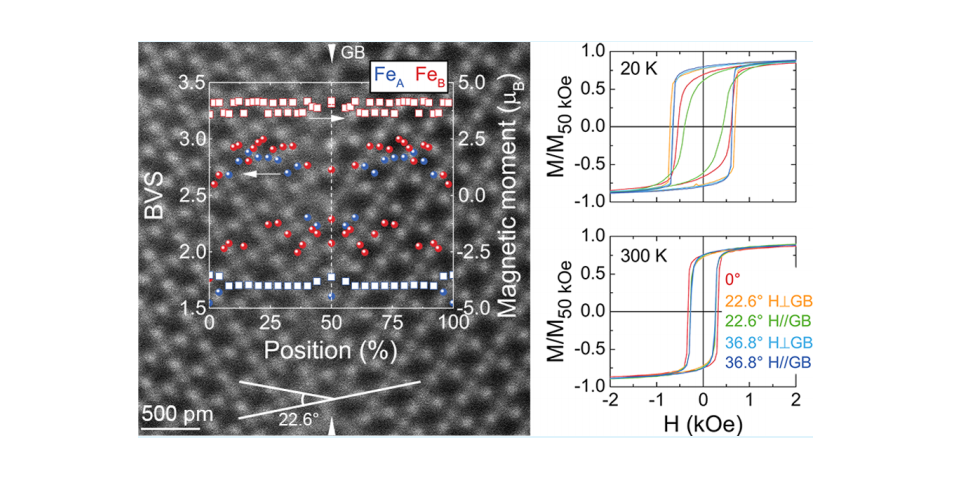
Grain Boundary Effects on the Magnetic and Transport Properties of Fe3O4 Bicrystal Films
The artificial grain boundaries (GBs) with different tilt angles are produced in Fe3O4 films using SrTiO3 bicrystal substrates. The saturation magnetization of Fe3O4 bicrystal films is enhanced. We probe the mechanism of GBs on the magnetic and transport properties, and show that strategies utilizing GBs can tune the physical properties of highly spin-polarized materials. (ACS Applied Materials & Interfaces 13(5): 6889-6896. (2021)) 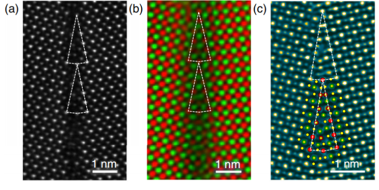
Two-Dimensional Room-Temperature Giant Antiferrodistortive SrTiO3
We created a two-dimensional antiferrodistortive (AFD) strontium titanate (SrTiO3) phase at room temperature. We found that such an anomalous room-temperature AFD phase with the thickness of approximate six unit cells is stabilized by the charge doping from oxygen vacancies. Our study also provided newstrategies to create low-dimensional anomalous elements for future nanoelectronics via grain boundary engineering. (Physical Review Letters, 126(22): 225702. (2021)) 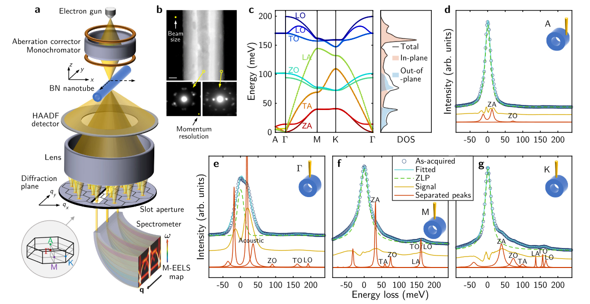
Four-Dimensional Vibrational Spectroscopy
Our group developed a four-dimensional electron energy loss spectroscopy (4D-EELS) technique using scanning transmission electron microscopy, which for the first time achieved phonon dispersion measurements at different positions in a single nanostructure. Using a slit diaphragm to collect scattered electrons on the diffraction plane, phonon spectra with different momentum transfer can be collected in parallel, which greatly improves the data collection efficiency, enabling two-dimensional scanning in space to record the phonon spectra at different positions at the same time. dispersion relation becomes possible. (Nature Communications, 12(1):1179. (2021)) 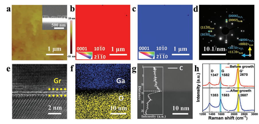
Preparation of nitride films with high Indium Composition
Nitride films high in indium (In) play a crucial role in the fabrication of indium-rich InGaN-based optoelectronic devices. To overcome the limitation that ln incorporation requires low temperature and dissociated nitrides, we propose a strain-modulated growth method, graphene (Gr)-nanorod (NR)-enhanced quasi-van der Waals epitaxy, to increase InGaN In composition in alloys. (Physical Review B 97(18):180103 (2018)) |

